
© 1996 IEEE. Personal use of this material is permitted. However, permission to reprint/republish this material for advertising or promotional purposes or for creating new collective works for resale or redistribution to servers or lists, or to reuse any copyrighted component of this work in other works must be obtained from the IEEE.
By choosing to view this document, you agree to all provisions of the copyright laws protecting it.
A VHDL Synthesis Model of the MIPS Processor for use in Computer Architecture Laboratories
JAMES 0. HAMBLEN, SENIOR MEMBER, IEEE
Abstract - This contribution describes and contains the necessary VHDL files to synthesize and simulate a MIPS 32-bit RISC processor core for use in introductory computer architecture classes. This MIPS processor core is based on the design presented in chapters 5 and 6 of the widely used text, Computer Organization & Design the Hardware/ Software Interface by David Patterson and John Hennessy. IEEE Standard Logic 1164 is used in the VHDL model and versions are provided for several popular CAD tools. Our experiences in using this model in our introductory computer architecture classes, CmpE 2510 and CmpE 3510, during the past two years are described along with typical laboratory assignments.
Introduction
Traditionally, undergraduate computer architecture laboratory courses have used special purpose software simulators to aid in the design and modeling of a simple computer. This model of a simple computer is used to explain and reinforce many of the new ideas presented in lectures. In recent years, many such courses have been based on behavioral or RTL level simulations only. A methodology is described using VHDL based rapid prototyping for top down hierarchical design, synthesis, and a full gate level timing simulation of a 32-bit RISC processor through the use of advanced CAD tools. These commercial CAD tools are available to universities at substantial educational discounts.
A VHDL synthesis based laboratory course was developed to accompany our undergraduate computer architecture course sequence. Computer and electrical engineering majors take this two-quarter course sequence. Our goal was to enable students to design and develop a realistic computer system simulation using many of the recent advances in CAD tools for logic synthesis and simulation. One of these recent developments, VHDL, Very High Speed Integrated Circuit Hardware Description Language, is now widely used to model and simulate digital circuits. VHDL has syntax similar to Pascal or ADA. VHDL Synthesis tools are available which automatically translate a high level VHDL behavioral model into a gate level digital logic schematic. Increasing the level of abstraction using such automatic synthesis tools produces substantial reductions in development time for complex digital circuits and is now widely used in industry.
II. Computer Architecture Design Laboratory
The required undergraduate computer architecture course sequence consists of two, four hour, one quarter courses, Computer Engineering 2510 and 3510. Computer and electrical engineering students at the Georgia Institute of Technology take these courses in sequence. The goals of this course sequence are to introduce students to assembly language programming, computer arithmetic, computer architecture and to provide an introduction to modern digital CAD tools. At the end of the sequence, students should have a basic understanding of computer operations from the high-level language programming level to the gate level implementation of the computer system. Students are already familiar with digital design, computer programming in a high level language, Field Programmable Gate Arrays, and VHDL based modeling and simulation of simple digital logic circuits from prerequisite courses.
Computer Architecture I and II is taught every quarter and has an enrollment of around 400 students per year. Course lectures are held three hours a week and three hours of laboratory work per week are required. Several tools such as assemblers, compilers, and CAD tools were collected from a variety of sources for this laboratory and many are available free of charge to educational users via the Internet. Links to many of these tools are included in the reference section. The lecture and laboratory outline for Computer Architecture I and II is shown in Table 1. The MIPS 32-bit RISC assembly language, integer and floating point computer arithmetic, and several hardware implementations of the MIPS processor are contained in the course textbook [1].
In Computer Engineering 2510, Computer Architecture I, students complete three assembly language programming laboratory assignments using SPIM, a MIPS assembler and instruction level simulator. SPIM is a public domain program available free via anonymous ftp for UNIX, PC and MAC platforms [1,2,3]. The first two assembly language program assignments demonstrate integer operations, control structures, stack operations, and subroutine linkage.
TABLE 1
Outline of Lecture and Laboratory Topics
|
Week |
Computer Architecture I
Laboratory Assignment |
Computer Architecture I
Lecture Topic |
|
1 |
SPIM tutorial |
MIPS RISC architecture |
|
2 |
First assembly lang. Program |
MIPS instruction Set |
|
3 |
" |
SPIM assembly language |
|
4 |
Second assembly lang. Program |
Stacks and subroutines |
|
5 |
MIPS C compiler |
Integer computer arithmetic |
|
6 |
MIPS floating point program |
Floating point arithmetic |
|
7 |
VHDL CAD tool tutorial |
Overview of VHDL |
|
8 |
VHDL synthesis and simulation running a new test program |
MIPS processor hardware implementation and VHDL model |
|
9 |
VHDL synthesis and simulation
adding a new instruction |
Modifying hardware and VHDL to add new instructions and features |
|
10 |
" |
Alternative microcoded MIPS |
|
Week |
Computer Architecture II
Laboratory Assignment |
Computer Architecture II
Lecture Topic |
|
1 |
VHDL CAD tool tutorial |
Overview of pipelining |
|
2 |
Pipelining the MIPS design |
Pipelining the MIPS hardware |
|
3 |
" |
Pipeline control problems |
|
4 |
Adding a hazard unit to the MIPS |
MIPS hazard detection hardware |
|
5 |
" |
MIPS forwarding unit |
|
6 |
Adding forwarding to the MIPS |
" |
|
7 |
" |
MIPS branch flushing |
|
8 |
Add branch flushing to the MIPS |
I/O devices and busses |
|
9 |
" |
Caches and virtual memory |
|
10 |
MIPS design on FPGA |
Introduction to parallel computers |
Students compare their hand written assembly code for the second assembly language program to the code generated by a C compiler that has compiled a program to perform the same operation. Lcc, a public domain retargetable C compiler, available free for UNIX workstations and PCs, is used for this step [4]. One of the target machines already supported by this compiler is the MIPS. MIPS assembly language source files generated by the compiler are then used by students to demonstrate compiler code generation. In the final assembly language program, students implement a floating-point function such as square root. The SPIM MIPS simulator supports floating-point instructions and operations. IEEE Standard 754 floating point format is used in the MIPS processor [1,2,3].
After the MIPS assembly language laboratory assignments, students have two laboratory assignments in which they modify a VHDL model of a MIPS RISC processor. A VHDL synthesis model of the MIPS was developed at Georgia Tech for use in this laboratory. VHDL source code for this model and instructions for several CAD tools are available using the link provided at the end of this paper. It should be noted that existing synthesis tools impose a number of restrictions upon the VHDL source code and require the use of a subset of standard VHDL. Most VHDL simulation models cannot be directly converted to a synthesis model since they use features not supported by the synthesis tools.
VHDL has a Pascal or ADA based syntax and it includes several extensions which make it useful for modeling of digital circuits [5]. VHDL processes and modules execute in parallel. The WAIT statement suspends a process until the specified condition is true. A WAIT statement which waits for the clock signal to change is used to model and synthesize latches and flip-flops. Another VHDL extension is the AFTER keyword. The keyword, AFTER, followed by a time delay can be used to model the physical time delays present in digital circuits. These features permit VHDL to model the parallel operation of digital hardware even including physical time delays, if so desired. Behavioral VHDL based modeling of digital systems has been in use for several years. VHDL based logic synthesis is a newer development. In VHDL synthesis models, the time delays in the synthesized schematic are automatically simulated using special libraries for the target logic technology.
An example of VHDL synthesis using the MIPS control unit is shown in Figs. 1 and 2. The VHDL source code is shown in Fig. 1 and the schematic automatically generated by the synthesis tool is shown in Fig. 2. The input to this module is the 6-bit instruction opcode, OP(5-0). The language support for standard logic vectors or arrays of bits, such as OP, greatly simplifies coding of the VHDL model. All busses and register values use the standard logic vector data type. It is possible to change the entire value of a vector with one assignment statement or to access smaller bit fields when needed. The outputs of this VHDL module are the various control signals used in the processor. The synthesis tool automatically performs logic minimization and multi-level logic synthesis. As an example, many of the intermediate level gate outputs are shared between the various output circuits shown in the schematic in Fig. 2. The original VHDL code had logic equations with six inputs for the opcode bits. More than two levels of gating are required for implementation, since the logic technology used for synthesis allows a maximum of four inputs per gate.
- -- control module (model of MIPS control module)
- library IEEE;
- use IEEE.std_logic_1164.all;
- entity control is
- port( signal Op : in std_logic_vector(5 downto 0);
- signal RegDst : out std_logic;
- signal ALUSrc : out std_logic;
- signal MemtoReg : out std_logic;
- signal RegWrite : out std_logic;
- signal MemRead : out std_logic;
- signal MemWrite : out std_logic; signal Branch : out std_logic;
- signal ALUop0 : out std_logic;
- signal ALUop1 : out std_logic);
- end control;
- architecture behavior of control is
- signal Rformat, Lw, Sw, Beq : std_logic;
- begin -- behavior of MIPS control
- Rformat <= ((NOT Op(5)) AND (NOT Op(4)) AND (NOT Op(3)) AND (NOT Op(2)) AND (NOT Op(1)) AND (NOT Op(0)));
- Lw <= (Op(5)) AND (NOT Op(4)) AND (NOT Op(3)) AND (NOT Op(2)) AND (Op(1)) AND (Op(0));
- Sw <= (Op(5)) AND (NOT Op(4)) AND (Op(3)) AND (NOT Op(2)) AND (Op(1)) AND (Op(0));
- Beq <= (NOT Op(5)) AND (NOT Op(4)) AND (NOT Op(3)) AND
- (Op(2)) AND (NOT Op(1)) AND (NOT Op(0));
- RegDst <= Rformat;
- ALUSrc <= Lw or Sw;
- MemtoReg <= Lw ;
- RegWrite <= Rformat or Lw;
- MemRead <= Lw ;
- MemWrite <= Sw ;
- Branch <= Beq ;
- ALUOp1 <= Rformat ;
- ALUOp0 <= Beq ;
- end behavior;
FIG. 1 VHDL Source Code for MIPS Control Unit.
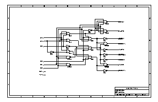
FIG. 2 Control Unit Schematic Produced by VHDL Synthesis.
New instructions and features are added to the VHDL model of the MIPS processor in the two VHDL based laboratory assignments. Detailed block diagrams of the MIPS processor architecture are presented in the course textbook [1]. Changes and additions to the block diagram are made as new instructions are added to the processor. Students determine the hardware changes or additions needed and modify the appropriate source code in the MIPS VHDL model. Typical assignments have included the addition of unconditional branch instructions and unsigned add operations. The entire design is resynthesized to a gate level schematic, and a gate level timing simulation running a short machine language test program is used to verify correct operation of the new instructions. An example timing diagram with the MIPS model running a short test program is shown in Fig. 3. Tutorial and batch command files are included to make the process simple enough for first time users of the CAD tools.
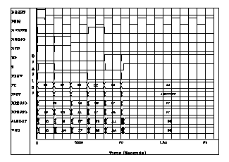
- FIG. 3 MIPS Timing Diagram Produced by VHDL Synthesis & Simulation.
Student's VHDL models are automatically synthesized into gate level logic and simulated using a popular commercial CAD tool, Viewlogic Workview Office for Windows NT/ 95. Several other VHDL based CAD synthesis tools could also be used such as Synopsys[6], Mentor, or Cadence; however, these are available only for UNIX platforms. Viewlogic's, Altera's and Xlinix's VHDL synthesis and simulation tools are currently available for UNIX or PC platforms at a substantial educational discount. Links for these CAD tools vendors can be found in the reference section of this paper. For the PC based CAD tools, a Pentium based PC with at least 32 megabytes of memory and 500 megabytes of available disk space is recommended. The tools will also run on older generation 486 machines but these require several minutes to run the complex synthesis and simulation tools. Synopsys CAD tools run on Unix workstations and several hundred megabytes of disk space are required to install the CAD tools. As seen in Fig. 4, we currently have seventy Pentium PC based machines with Viewlogic, Xilinx and Alterra CAD tools available for student use in this laboratory. In addition to class handouts, several VHDL references are provided and a full set of CD-ROM on-line documentation for the VHDL CAD tool is available via a shared network drive [7,8]. The Xlilinx 4000 ASIC, Application Specific Integrated Circuit, technology library is used for gate level synthesis and timing information [8]. With minor changes it is possible to resynthesize using other ASIC technologies. Gate count and timing information is automatically reported by the synthesis tool.
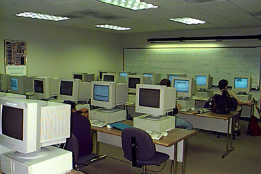
- FIG. 4 Computer Architecture CAD Laboratory.
VHDL synthesis tools have predefined VHDL based implementations of adders, subtractors, and making the design process easier. Hardware for addition and subtraction can be automatically generated by operator inferencing in the VHDL code. With current VHDL synthesis tools, IEEE Standard Logic 1164 is the most widely used standard. Some portions of the VHDL model would need to be modified if a different VHDL synthesis CAD tool is used. Typically, only small changes are needed in the library and use statements at the beginning of each source code module to convert to a different CAD tool that supports VHDL Synthesis and IEEE Standard Logic 1164. It is possible for students to examine the synthesized schematics and to experiment with different hardware design tradeoffs such as time and area. When running simulations, a timing diagram can be produced and with some CAD tools it is also possible to back annotate the schematics with simulation values to aid in debugging.
Machine language test programs can be hand assembled, assembled using the SPIM assembler, or even produced using the C compiler. This machine language file is then read into the VHDL model's memory with a read command or hardcoded into a VHDL synthesized ROM used to simulate instruction memory. On current generation PCs, the entire synthesis process for the smaller model requires just a few minutes of computer time. Approximately 3,700 gates are used to implement the basic MIPS VHDL model. After student modifications that add new features, the improved pipelined MIPS processor uses approximately 6,000 gates.
In Computer Engineering 3510, Computer Architecture II, students study pipelining techniques, caches, virtual memory, and I/O hardware. In five laboratory assignments, students modify the synthesizable VHDL model to create an improved MIPS RISC processor with pipelining. In the first laboratory assignment, students pipeline the existing MIPS VHDL model. The VHDL model contains separate modules for each of the five MIPS pipeline stages making the student pipelining process much easier. In this assignment, students add the pipeline registers to each stage or module and modify the control unit. A top-level VHDL structural model is used to connect the five stages together. This structure generates two levels of hierarchy in the design. Breaking up the model into different pipeline stages makes the model much easier to understand and to synthesize. The textbook contains detailed block diagrams of the pipelined MIPS processor[1]. Instructions are traced one clock cycle at a time as they move through the pipeline stages and the value of all busses and control signals are shown in a detailed set of diagrams. Short machine language test programs identical to those presented in the course textbook are run in the simulator to verify correct operation. Using the simulation output, a timing diagram with bus values indicated in hexadecimal, students can check the computer's operation against the textbook's diagrams to verify correct operation. On the PC platform, the VHDL gate level timing simulator can execute the MIPS test programs in a few seconds.
Automatic pipeline stalling using a hazard detection unit is added to the pipelined MIPS VHDL model in the second laboratory assignment. The textbook modifies the control unit to detect a data hazard between instructions in the pipeline and to stall or wait a clock cycle. An example data hazard would be an instruction in the pipeline that writes a register that is then read by the instruction that immediately follows it. The pipelined register write occurs after the read operation for the next instruction and the incorrect register data value would be used. This problem is solved by stalling and later by forwarding. These problems are carefully avoided by the MIPS machine language test programs until they are discussed in the textbook and corrected by adding additional hardware.
Forwarding is added between the pipeline stages to reduce the number of stalls in the third laboratory assignment. As outlined in the textbook, two forwarding multiplexers are added to the ALU inputs along with a more complex control unit that selects the appropriate input when it detects a data hazard. In the case of a register data hazard, the new value of the register is supplied to the ALU by the forwarding multiplexer before it is written back to the register file.
Branch flushing is added to the pipelined MIPS VHDL model in the fourth assignment. When a branch is taken several instructions after the branch are already in the pipeline and they must be automatically cleared out of the pipeline or flushed. The control unit and pipeline registers are modified to detect a branch flush operation and to clear the appropriate pipeline registers to avoid executing unwanted instructions already in the pipeline.
Additional features such as a cache, exception handling hardware, or a different branch instruction scheme are added to the pipelined MIPS VHDL mode in the final laboratory assignment. On the MIPS processor exceptions, such as overflow, save the current PC in a special register and jump to a trap address. In each laboratory assignment, complete synthesis of the design to gate level, followed by a full gate level timing simulation is used to execute short machine language test programs.
Many students encounter timing problems present in their VHDL models that cause errors in the VHDL gate level timing simulation. In every case, it was a real timing problem traced back to VHDL coding errors. They were able to detect and diagnose the problem using the simulation, modify the VHDL model, resynthesize, and eliminate the timing problems. Problems included uninitialized values in flip-flops, combinatorial loops, gating signals with the clock, and logic hazards on critical write control lines. These real world problems familiar to most experienced digital designers are not detected by most RTL or VHDL behavioral simulations.
VLSI chip designs with higher clock rates could be automatically produced using the VHDL synthesis generated schematic or netlist as the input to a silicon compiler [9]. The Lager silicon compiler automatically generates a standard cell layout. Interfaces to this tool have been developed for synthesized designs using Viewlogic VHDL. This tool is available upon request for UNIX platforms free of charge to educational users. In theory, a MIPS VLSI processor chip could then be fabricated using a VLSI fabrication service. The actual fabrication process would be costly and would add a substantial delay due to VLSI fabrication times. Actual fabrication of the chip would make design turnarounds difficult, if not impossible, in a one quarter course. It is also possible to fit the entire MIPS VHDL synthesized design into a large Xilinx FPGA chip such as a 4005 [8], Altera FPGA chips such as an EPM9400[12], or onto several automatically interconnected FPGA chips in a hardware emulation device [10,11]. An earlier version of the laboratory using older generation PC based CAD tools prior to the introduction of IEEE Standard Logic 1164 for VHDL is described in [13]. Hardware emulation with designs in the range of 10,000 to 30,000 gates has also been used in a more advanced computer architecture laboratory design course, Computer Engineering 4500 [14].
- III. MIPS Synthesis Model
Source files for the VHDL Synthesis model of the MIPS processor core from [1] are included with this paper. Versions are available for Viewlogic, Alterra, and Synopsys CAD tools. A link is provided at the end of this paper. When required, synthesis and simulation batch files are also included with each version. These files are stored in zip file format, so an unzip utility, such as pkunzip or WinZip is required. Some portions of the VHDL model would need to be modified if a different VHDL synthesis CAD tool is used. Typically, only small changes are needed in the library and use statements at the beginning of each source code module to convert to a different CAD tool that supports VHDL Synthesis and IEEE Standard Logic 1164.
A full 32-bit version of the MIPS requires several hours to synthesize on the PC platform. A smaller version with an 8-bit data path with full 32-bit instructions and control was developed to permit the design to synthesize and simulate in just a few minutes for student laboratory assignments. This version has minimal VHDL source level modifications from the 32-bit version. Changes are limited to the bit vector array size declarations for variables and signals in the data path. If fast systems are available and long run times are not an issue, the width of the data path could be easily changed back to 32-bits. The smaller model requires machine language test programs that use 8-bit integer values. Since the hardware test programs in the textbook are just a few instructions long and relatively simple, this has not affected the pedagogical value of the MIPS VHDL model.
A two level hierarchy is used in the model. TOP_SPIM.VHD is the top level of the hierarchy. It consists of a structural VHDL model that connects the five behavioral modules. The five behavioral modules are already setup so that they correspond to the different pipeline stages for the MIPS. This makes it much easier to modify when the model is pipelined by students in assignments. For many synthesis tools, a hierarchy is also required to synthesize large logic designs. IFETCH.VHD is the sub module which contains instruction memory and the program counter. CONTROL.VHD contains the logic for the control unit. IDECODE.VHD contains the dual ported register file. EXECUTE.VHD contains the data and branch address ALUs. DMEMORY.VHD contains the data memory.
- IV. Conclusions
Using current generation CAD tools it is possible for undergraduate students to design and develop working simulations of complex computer systems as part of their laboratory work even in introductory courses. VHDL synthesis and simulation provides a new paradigm for computer architecture classes. The equipment and CAD tools required are available to schools at prices comparable to existing instructional laboratories. Rapid prototyping of the design using synthesis and simulation in the laboratory demonstrates and unifies many of the ideas taught in numerous undergraduate classes and serves as an ideal laboratory course for introductory computer architecture students. Students have a better understanding of pipelining now that they see the problems in their laboratory assignments. Feedback from industry and graduates has been very positive on the adoption of widely used commercial CAD tools. Several of our graduates have reported that they are using the same CAD tools and FPGAs in their current jobs and feel it was a very beneficial experience to have used them in the computer architecture classes. More advanced courses spend less time on basic CAD tool training and VHDL since students now have that experience in a lower level required course. Students gain a sense of accomplishment and are motivated to work harder on the computer design projects when given the opportunity to use advanced general purpose CAD tools with realistic timing and gate level simulations rather than a special purpose computer simulation program.
Click here to obtain source code for MIPS VHDL Model
- Click here to obtain copy of course materials in MS Word format.
Acknowledgments
Donations of Personal Computers from Intel, and CAD tools from Viewlogic, Xilinx, and Altera made the development of this new laboratory possible. The author would also like to thank the many students and teaching assistants who aided in the development of this new laboratory. A grant from the Georgia Tech Foundation enabled the purchase of additional software and equipment needed for the laboratory.
- References
[1] Patterson, D. and Hennessy, J., Computer Organization & Design The Hardware/Software Interface, San Mateo, CA: Morgan Kaufmann, 1994. Information available from http://www.mkp.com
[2] Larus, J., Assemblers, Linkers, and the SPIM Simulator, University of Wisconsin, 1991. Reprinted in [1], manual and SPIM software available via ftp from ftp.cs.wisc.edu.
[3] Kane, G, and Heinrich, J., MIPS RISC Architecture, Englewood Cliffs, N.J.: Prentice Hall, 1992. Information available from http://www.prenhall.com.
[4] Fraser, C., and Hanson, D., A Retargetable C Compiler: Design and Implementation, Redwood City, CA: Benjamin/Cummings Publishing, 1995. Information and compiler source code available from http://www.cs.princeton.edu/software/lcc
[5] Ashenden, P., The VHDL Cookbook, University of Adelaide, 1990. Available via ftp from bears.ece.ucsb.edu.
[6] Kurup, P., and Abbasi, T., Logic Synthesis Using Synopsys, Boston, Mass: Kulwer Academic Publishers, 1996. Synopsys information available from http://www.synopsys.com
[7] VHDL Reference Manual for Synthesis, Marlboro Massachusetts: Viewlogic Systems, 1994. Viewlogic information available from http://www.viewlogic.com
[8] XACT Viewlogic Interface User Guide, San Jose, CA: Xilinx Corporation, 1996. Xilinx information available from http://www.xilinx.com .
[9] Brodersen, R.W., editor, Anatomy of a Silicon Compiler, Boston, Mass: Kulwer Academic Publishers, 1992. Lager information available from http://infopad.EECS.berkeley.edu/research/tools/lager
[10] Owen, H., Khan, U., and Hughes, J., "FPGA Based Emulator Architectures", More FPGAs (Will Moore and Wayne Luk, Eds.), Abbingondon, England: Abbingondon EE & CS Books, pp. 399-409 (1994). Emulator Information available from http://www.zycad.com and http://www.quickturn.com
[11] Khan, U., Owen, H., and Hughes, J., "FPGA Architectures for ASIC Hardware Emulators," Proceedings of the Sixth Annual IEEE International ASIC '93, New York, pp. 336-340, October 1993.
[12] ALTERA MAX+PLUS II Getting Started, San Jose, CA: Altera Corporation, 1996. Altera information available from http://www.altera.com
[13] Hamblen, J., Using VHDL Based Modeling, Synthesis, and Simulation in an Introductory Computer Architecture Laboratory, International Journal of Electrical Engineering Education, vol. 33, no. 3, pp. 251-260, July 1996.
[14] Hamblen, J., Owen, H. L., and Yalamanchili, S., "Introduction of Rapid Systems Prototyping into Undergraduate Computer Engineering Curricula," Proceedings of the Twenty Fifth Annual ASEE Frontiers in Education Conference, Atlanta, GA., November 1995. Available from http://fre.www.ecn.purdue.edu/fre/asee/fie95
Contact Information
JAMES 0. HAMBLEN
School of Electrical and Computer Engineering
Georgia Institute of Technology
Atlanta, Georgia 30332-0250
Phone: 404-894-3027
Fax: 404-894-9959
E-mail: hamblen@ece.gatech.edu
Biographies
James O. Hamblen is an associate professor in electrical and computer engineering at Georgia Tech. He received his Ph.D. in electrical engineering from Georgia Tech in 1984. His other degrees include an M.S.E.E. from Purdue University and a B.E.E. from Georgia Tech. Prior to returning to Georgia Tech to work on his Ph.D., he worked as a systems analyst for Texas Instruments in Austin, Texas, and as a senior engineer for Martin Marietta in Denver, Colorado. Professor Hamblen's current research interests include rapid prototyping, high-speed parallel and VLSI computer architectures, computer-aided design, and reconfigurable computing.